How does a PbS photoconductive detector work?
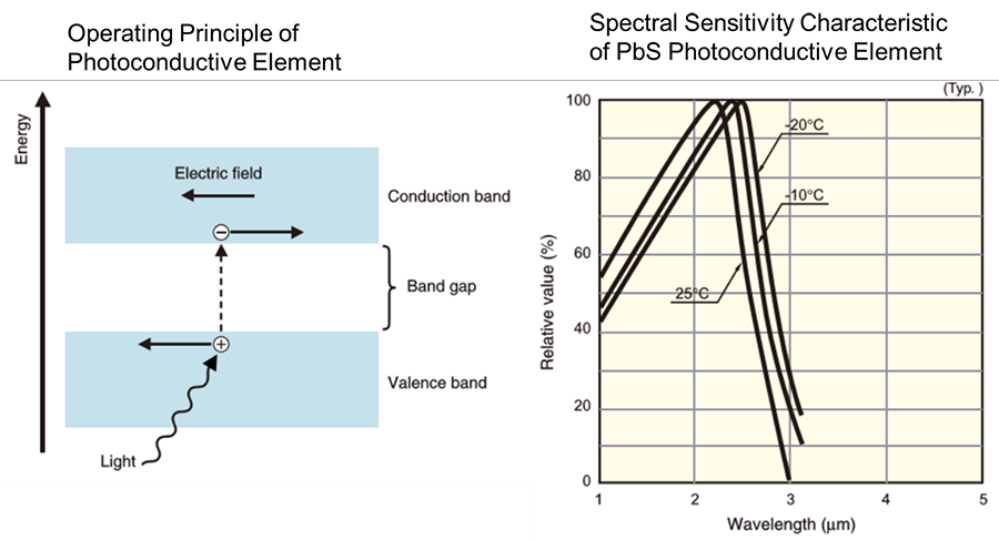
A photoconductive element is a photoelectric conversion element that utilizes the phenomenon of photoconduction, whereby the electrical conductivity (resistance) of a material changes when it is irradiated with light. The figure on the left illustrates the operating principle. When light of energy greater than the energy gap between the conduction band and the valence band strikes the element, electrons in the valence band are excited into the conduction band, and holes are created in the valence band. With a PbS photoconductive element, the resistance is reduced in accordance with the intensity of incident light, and this is obtained as a signal using an external circuit.
If the element is cooled, the spectral sensitivity characteristic shifts to the long-wavelength end; as a result, the element becomes more sensitive to longer wavelengths. At the same time, however, the response speed decreases. Although PbS photoconductive elements can, unlike some other near- infrared detection elements, be used at room temperature, they are still delicate elements for which the sensitivity, response speed, and dark resistance change according to the temperature. The graph on the right shows the spectral sensitivity characteristic of a PbS photoconductive element. Note the wavelength axis is in micrometers, so 1 micrometer is equal to 1000 nanometers.