Graphene and Other 2D Materials
Testing, Analysis and Inspection of Graphene and Other 2D Materials
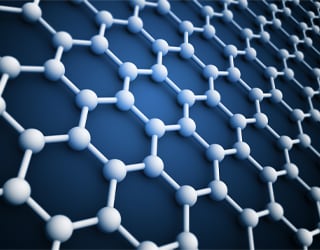
Graphene, a single-layer sheet of carbon atoms arranged in a honeycomb structure, has been hailed as a wonder material for its extraordinary combination of mechanical, electrical, optical, and thermal properties, and its ability to impart those properties to other materials. Since its discovery, graphene has spawned a rapidly expanding field of research into monolayer or “two-dimensional” materials – other examples include borophene and molybdenum disulfide – and researchers have incorporated these exceptional materials into an ever-growing list of potential applications, including composites, electronics, energy storage, energy harvesting, sensors, coatings, filtration, and more.
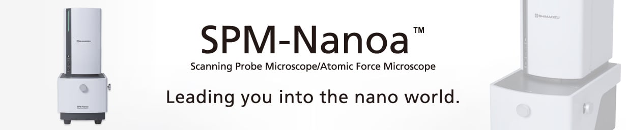
The investigation and characterization of such materials requires sensitive instrumentation to examine their atomic-level properties and interactions. Shimadzu Scanning Probe Microscopes (SPM) use nanometer-sized probes to scan the surface of samples, creating images of their topology and local properties. Kratos surface analysis instruments utilize X-ray Photoelectron Spectroscopy and several other spectroscopic techniques to offer high-sensitivity and high-resolution analysis of chemical composition and chemical shifts with unrivaled automation and sample handling features.
Featured Applications
Building the energy level diagram of a 2D material using coincident UPS and IPES
Understanding the nature of the electronic configuration and properties of these materials is important for their development. Conventional methods to analyze 3D materials struggle to determine the properties for ultra-thin films, and these thin layers are what exhibit the revolutionary properties. Using a combination of the surface sensitive techniques Inverse Photoelectron Spectroscopy (IPES) and Ultraviolet Photoelectron Spectroscopy (UPS), however, we demonstrate how the analyst can obtain information on the nature of the electronic properties for single and multi-layer stacks. In this example the properties of a thin layer of MoS2 are investigated. Bulk MoS2 is a diamagnetic, indirect bandgap semiconductor similar to silicon, with a bandgap of ~1.2 eV. However, with reduced thickness the bandgap increases [1,2], with a confinement-induced shift of the indirect gap from the bulk value. Thickness/growth control is therefore critical to the performance of this material in next-generation devices.
Graphene - macro/microscopic imaging and thickness metrology
Here we analyze graphene flakes deposited on a 10 mm x 10 mm piece of Si wafer with a 100 nm thick oxide overlayer. The motivation was to determine the distribution, shape and thicknesses of particular flakes of interest and to illustrate the application of XPS as a metrological tool for these materials.