AABC (Advanced Automotive Battery Conference) 2025
December 9-11
Caesars Palace
Las Vegas, NV
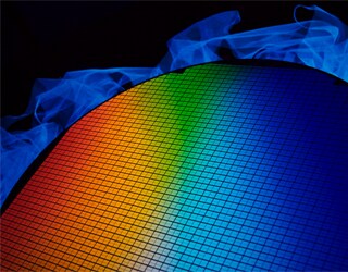
Shimadzu provides a range of analytical instruments to assist in the development and production of advanced electronics and semiconductor materials. Shimadzu SMX 225CT non-destructive x-ray tomography system, EPMA 8050G Electron Microprobe and SPM 8700 Scanning Probe Microscope are used world-wide to image the electronic materials that are critical to consumer electronics, transportation and communications industries.
Both inorganic and organic analyses are indispensable for electronics industry and related chemical industries. Purposes for analysis are wide ranging, and data generated can give much insight for research/development, reduction of defects, conforming to regulations and increasing productivity, all of which will contribute to delivering better products to consumers with diminished impact on our environment. This application handbook is a compilation of case studies where analytical techniques are playing critical roles in various parts of electronic industries. It demonstrates the range of analytical solutions provided by Shimadzu, from simple evaluation test to combinatorial use of inorganic and organic analytical methods. We are hoping that you will find the solution that addresses your needs.

In the electronics industry of recent years, solder joining technology has become increasingly important due to the miniaturization of electronic components and popularization of lead-free (Pb-free) solder. This article introduces the high resolution X-ray images which are possible only with FEEPMA ™ and the difference in the distribution of microparticles when the accelerating voltage is changed based on an example in which a solder joint on a printed circuit board implemented with a lead-free solder (Sn-3.0Ag-0.5Cu) was analyzed using an EPMA-8050G EPMA electron probe microanalyzer.
Cars equipped with these electronic devices vibrate constantly while in operation, and are also affected by temperature changes due to the atmospheric temperature and heat from the engine and road. Normal operation is necessary even in this severe environment. Since reliability requirements are high, ECUs and other electronic devices are almost always enclosed in cases, but this means it is not possible to inspect the devices themselves from their external appearance. Thus, nondestructive inspection by Xray techniques is required. This article introduces an example of observation of an ECU by using an X-ray CT system.
When CT images of digital camera lenses are obtained, the CT images often include lens artifacts that make it difficult to observe the assembly status. However, this problem can be solved by modifying the orientation of the lens being scanned by the CT system. This example describes the use of a Shimadzu microfocus X-ray CT system to observe a digital camera lens.
Foreign matter on printed circuit board patterns was analyzed using an electron probe microanalyzer (EPMA). It can be seen that copper has migrated from the cathode (negative) to the anode (positive). A distribution of chlorine (Cl) can also be confirmed at almost the same position as the copper (Cu).
Before measuring life time properties it is also important to measure the particle size distribution from the additive material, this can be measured with SALD-2300. Measurements in a range from 17 nm up to 2500 µm. With the rise of metal powder-based additive manufacturing and its acceptance for critical applications, it has become important to understand the behavior of the raw materials used in different AM Techniques.
This article introduces three example analyses: analysis of EVA film subjected to intense UV irradiation using a UV (ultraviolet) -Py (double-shot pyrolyzer) / GC-MS (gas chromatograph mass spectrometer) system, evolved gas analysis by mass spectrometry (EGA-MS) of EVA film which was degraded by UV irradiation in the same way as with the above, and analysis of the same using a Fourier transform infrared spectrophotometer (FTIR).